
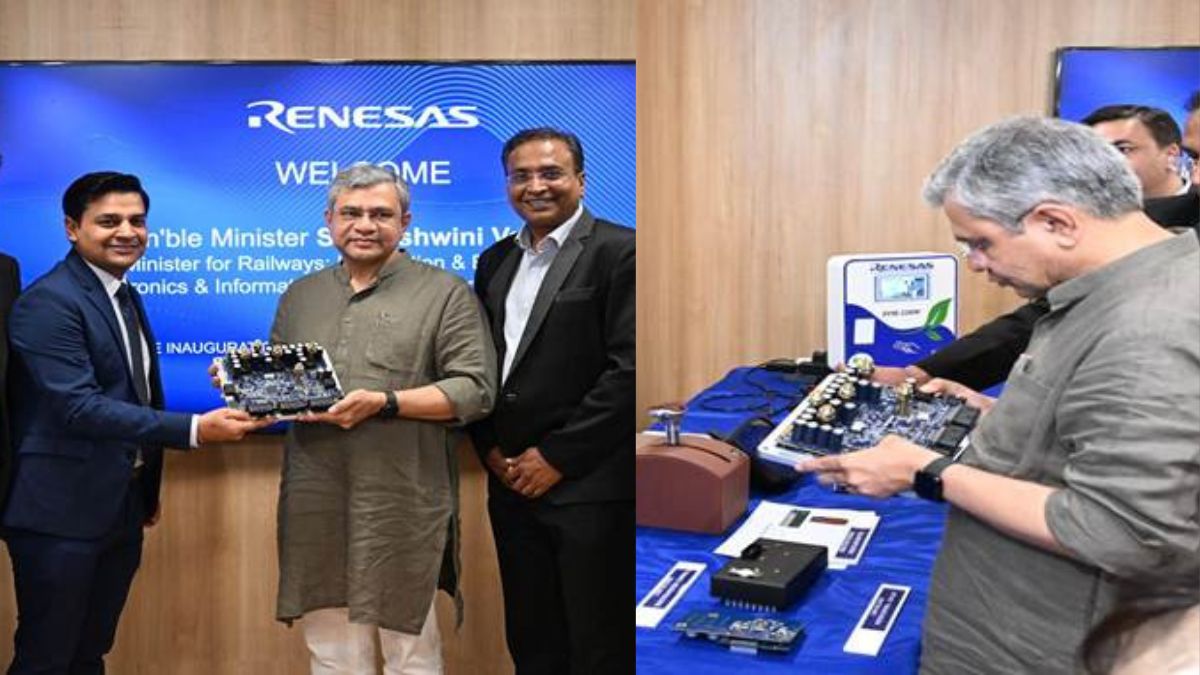
In a landmark moment for India’s semiconductor ambitions, Union Minister Shri Ashwini Vaishnaw inaugurated the country’s first 3nm chip design centres in Noida and Bengaluru. Set up by Renesas Electronics India, these state-of-the-art facilities represent a transformative leap in India’s chip design capabilities, aligning with the nation’s vision of becoming a global semiconductor powerhouse under the Aatmanirbhar Bharat mission.
Why in News?
India has entered a new frontier in semiconductor design with the inauguration of its first 3nm chip design centres. The move highlights the country’s growing prowess in advanced chip technology and supports its efforts to build a robust, end-to-end semiconductor ecosystem. This also supports India’s ambition to meet rising global and domestic demand for electronics through self-reliance and innovation.
Key Objectives and Highlights
- Launch of 3nm Chip Design Centres: Two facilities were inaugurated in Noida and Bengaluru by Union Minister Shri Ashwini Vaishnaw.
- First-of-its-kind in India: These centres are the first in India to design chips at the advanced 3nm node—marking significant technological progress from earlier 5nm and 7nm designs.
- Powered by Renesas Electronics India Pvt. Ltd.: A leading global embedded semiconductor solutions provider.
Government’s Semiconductor Push
- Holistic Strategy: India’s approach includes chip design, fabrication, ATMP (Assembly, Testing, Marking, and Packaging), and supply chain development.
- Global Recognition: Industry optimism has grown, evidenced by support from companies like Applied Materials and Lam Research.
- Academic Support: Over 270+ institutions have received EDA software tools and will now receive semiconductor learning kits to foster hands-on learning.
- Skill Development: A new semiconductor learning kit is being launched to develop industry-ready engineers.
Strategic Importance
- Geopolitical and Economic Value: The chip centres align with India’s strategic interests and Indo-Japan collaboration.
- Sustainable Growth: The initiative aims to build a self-reliant chip ecosystem, supporting manufacturing in smartphones, medical devices, automobiles, defense, and more.
Renesas’ Role and Vision
- Global Expertise: Renesas excels in embedded systems and system-level innovation.
- India Strategy: Plans to expand design capabilities from architecture to testing in India.
- Partnership with Academia and Startups: Through schemes like Design Linked Incentive (DLI) and Chips to Startup (C2S).
| Summary/Static | Details |
| Why in the news? | Ashwini Vaishnaw Inaugurates First 3nm Semiconductor Design Hubs in Noida and Bengaluru |
| Event | Inauguration of India’s first 3nm chip design centres |
| Inaugurated By | Union Minister Shri Ashwini Vaishnaw |
| Locations | Noida and Bengaluru |
| Organization | Renesas Electronics India |
| Significance | Marks India’s entry into next-gen 3nm chip design space |
| Government Initiatives | India Semiconductor Mission, DLI, C2S, semiconductor learning kits |
| Industry Partnerships | Renesas, Applied Materials, Lam Research |
| Educational Institutions Involved | 270+ colleges with access to EDA tools and learning kits |


 What Is Vantara University? India’s Firs...
 Mundra Port Sets Record as India’s Large...
 Former Delhi HC Judge Yashwant Varma Ten...