
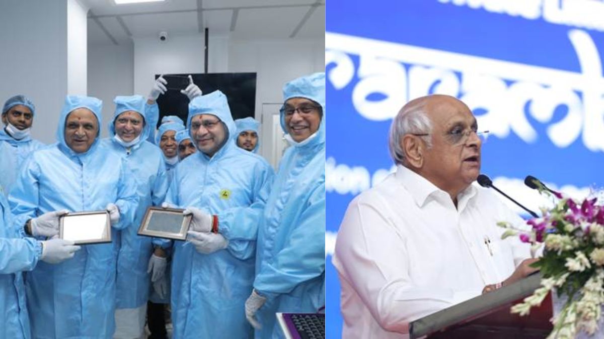
Union IT Minister Shri Ashwini Vaishnaw and Gujarat Chief Minister Shri Bhupendra Patel inaugurated one of India’s first full-scale Outsourced Semiconductor Assembly and Test (OSAT) Pilot Line Facilities in Sanand, Gujarat. Developed by CG Semi, this facility marks a major leap in India’s semiconductor roadmap and aligns with the broader vision of Atmanirbhar Bharat and technological sovereignty. With a growing global demand and an anticipated shortage of one million semiconductor professionals by 2032, India is positioning itself as both a production and talent hub in this strategic sector.
India Semiconductor Mission: A Turning Point
- The launch of the CG Semi OSAT facility is a cornerstone achievement under the India Semiconductor Mission (ISM). The OSAT Pilot Line will support chip assembly, packaging, testing, and post-test services, enabling faster qualification and paving the way for full-scale commercial manufacturing by 2026.
- The OSAT line represents a critical downstream segment in the chip supply chain. Its ability to process both traditional and advanced chip packages strengthens India’s aim of becoming a global semiconductor player.
- So far, the ISM has approved ten semiconductor projects, underscoring the government’s firm commitment to establishing a robust and self-reliant ecosystem.
Gujarat: The Emerging Silicon State
- Gujarat is at the forefront of India’s semiconductor mission. The state’s proactive policies, infrastructure readiness, and leadership support have positioned it as a pivotal node in India’s semiconductor revolution.
- CG Semi’s commitment includes an investment of over ₹7,600 crore (USD 870 million) to build two state-of-the-art plants—G1 and G2—over the next five years. The G1 facility, inaugurated today, will operate at 0.5 million units per day, while the G2 plant, under construction, will expand capacity to 14.5 million units daily by the end of 2026.
- Together, these facilities are expected to generate over 5,000 direct and indirect jobs, contributing significantly to local employment and high-tech skill development.
Empowering Talent and Academia
- The government has partnered with 270 universities and provided them with state-of-the-art semiconductor design tools, which saw over 1.2 crore usages in 2025 alone.
- As a direct result, 20 student-designed chips from 17 academic institutions have already been fabricated at the Semi-Conductor Laboratory (SCL), Mohali. This initiative is designed to fill a critical gap, with the world expected to face a shortage of 1 million semiconductor professionals by 2032.
- India aims to become the world’s largest semiconductor talent base, preparing a skilled workforce capable of sustaining the industry’s exponential growth.
Strategic Industry Collaboration
- CG Semi is a joint venture involving CG Power and Industrial Solutions (Murugappa Group), Renesas Electronics (Japan), and Stars Microelectronics (Thailand). This partnership brings global expertise to Indian soil, enabling technology transfer and rapid scale-up.
- To ensure operational excellence, Indian engineers and technicians have undergone hands-on training in Malaysia, sharpening their skills for high-volume chip assembly and testing operations.
- The plant features high-yield equipment, Manufacturing Execution Systems (MES) for automation and traceability, and labs for failure analysis and reliability testing. It is now undergoing ISO 9001 and IATF 16949 certification processes, with customer qualification runs set to begin soon.

 Parliament Rejects Impeachment of Chief ...
 Against All Odds: Indian Cyclist Divya S...
 India’s Most Advanced Atomic Reactor Att...