
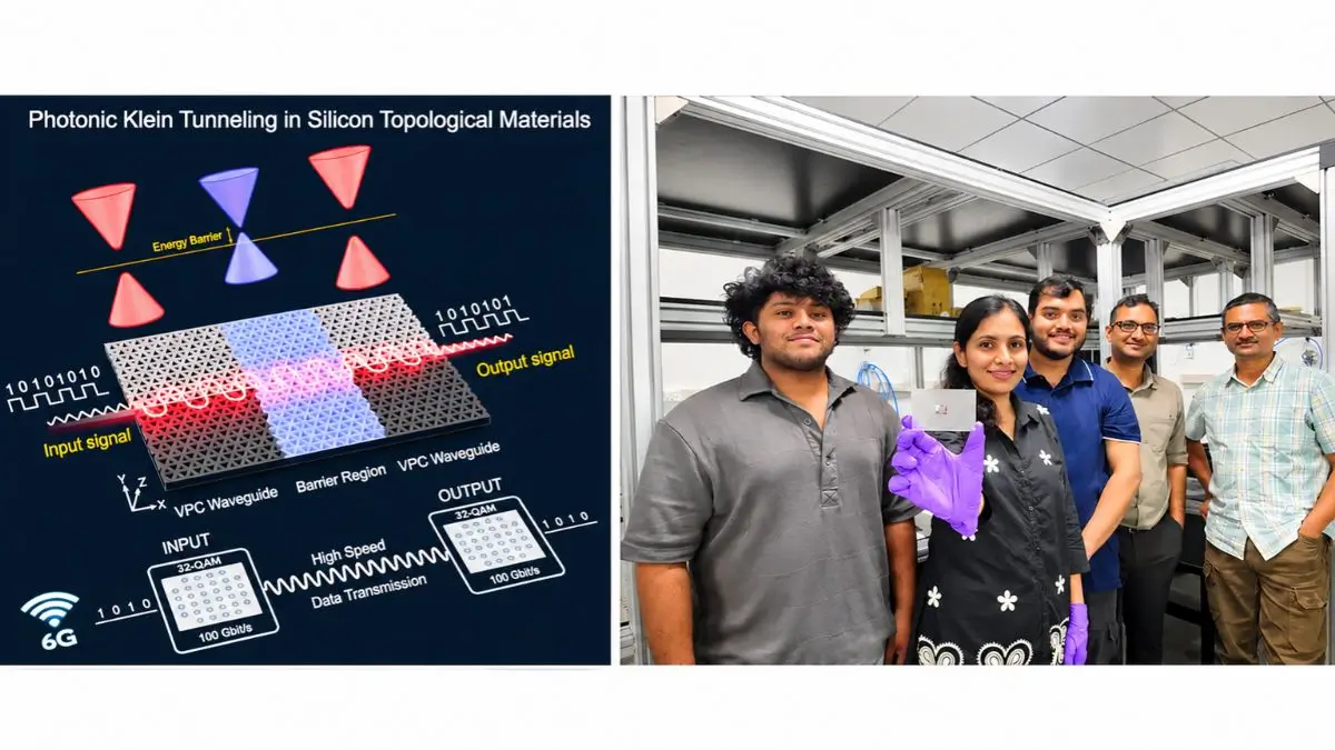
Researchers based at the Jawaharlal Nehru Center for Advanced Scientific Research (JNCASR) have developed a silicon chip capable of transmitting terahertz waves around designed obstacles with very little signal loss. In lab experiments, they were able to achieve data transfer rates of up to 100 gigabits per second (Gbps). This has been achieved using topological photonics and could help develop high-speed, compact communication circuits for 6G in the future.
How Does the Silicon Chip Work?
The research uses topological photonics, a field that studies how the structure of a material can guide and protect the movement of light or electromagnetic waves.
The researchers designed a silicon photonic crystal containing triangular holes arranged in a pattern resembling the honeycomb lattice of graphene. This structure guides terahertz waves along the boundaries between different regions and helps resist certain types of signal backscattering.
They created an artificial barrier by changing the sizes of triangular holes along a short section of the waveguide. Instead of losing a significant amount of energy at this obstacle, the terahertz waves continued to pass through it.
This phenomenon is known as photonic Klein tunneling. It is inspired by the Klein tunnelling effect in the area of quantum physics, in which certain particles can pass through potential barriers that would normally obstruct them.
Key Experimental Findings
The researchers fabricated total three devices using high-resistivity silicon, which is compatible with established semiconductor manufacturing processes.
| Device tested | Configuration | Data transmission speed |
| Double-barrier device | Two consecutive engineered barriers | 48 Gbps |
| Omega-shaped device | Four sharp bends and a central barrier | 60 Gbps |
| Power splitter | Barrier in one of its two branches | 100 Gbps |
Other important findings include,
- A single engineered barrier caused only just around 1-2% signal loss.
- Two consecutive barriers resulted in approximately 2–3% signal loss.
- Measurements were conducted across the 310–360 GHz.
- The power splitter achieved 100 Gbps using QAM-32 modulation which encodes information through variations in signal amplitude and phase.
- The two output signals of the splitter remained nearly identical.
At 100 Gbps, a 5 GB high-definition film could theoretically be transferred in less than half a second under ideal conditions.
What Are Terahertz Waves?
Terahertz (THz) waves are the electromagnetic waves that lie between the microwaves and infrared radiation in the electromagnetic spectrum.
- Frequency range: Commonly associated with approximately 0.1-10 THz.
- High bandwidth: Their high frequencies offer the potential for transmitting large amounts of data.
- Applications: High-speed wireless communication, imaging, spectroscopy, sensing and scientific research.
- Major challenge: Their transmission can be affected by signal scattering, reflection and atmospheric absorption, while guiding them through compact circuits is difficult.
The researchers tested their chip in the 310–360 GHz frequency range, which falls within the terahertz band.
Significance for Future 6G Networks
6G mobile communication will allow for much faster data transfer rates, reduced delays and increased network capacities.
One of the ways being looked at to increase bandwidth is using terahertz frequencies. However, creating compact circuits for efficient transmission is a challenge.
This research could help create,
- Fast data transfer using terahertz circuits.
- Low signal loss as signals can go through barriers and sharp corners.
- Compact photonic devices as all the signal routing and splitting can be done on a single silicon chip.
- Using advanced semiconductor technology as silicon is compatible with conventional semiconductor fabrication methods.
The team are looking to develop barriers that can be controlled using electricity, heat and mechanical means to route signals to different routes.
This research is an example of how this technology could work in future 6G systems. However, it does not mean that current 6G networks are available commercially or that consumers can get 100 Gbps wireless services.
About the Research Institution and Team
This research was conducted at the Jawaharlal Nehru Centre for Advanced Scientific Research (JNCASR), Bengaluru it is an autonomous institute under the Department of Science and Technology (DST), Government of India.
- Research leader: Dr Abhishek Kumar, Assistant Professor and head of the Meta Optics Laboratory (MetoLab), JNCASR.
- Joint first authors: Samina Mulla and Sangram Kumar Sadhu.
- Indian collaborators: Researchers from JNCASR, IISER Kolkata and IIT Bombay.
- International collaborators: Researchers from A*STAR, Singapore, and the University of Lille and CNRS, France.
- Research journal: Advanced Materials.
- Publication date: 11 October 2026.
- Research paper: Photonic Klein Tunnelling in Silicon Topological Materials for Terahertz 6G Interconnects.








 Aditya-L1 Reveals Asymmetric Expansion o...
 IndiaAI Mission Releases Indigenous AI F...
 ISRO Successfully Launches GSLV-F18 with...