
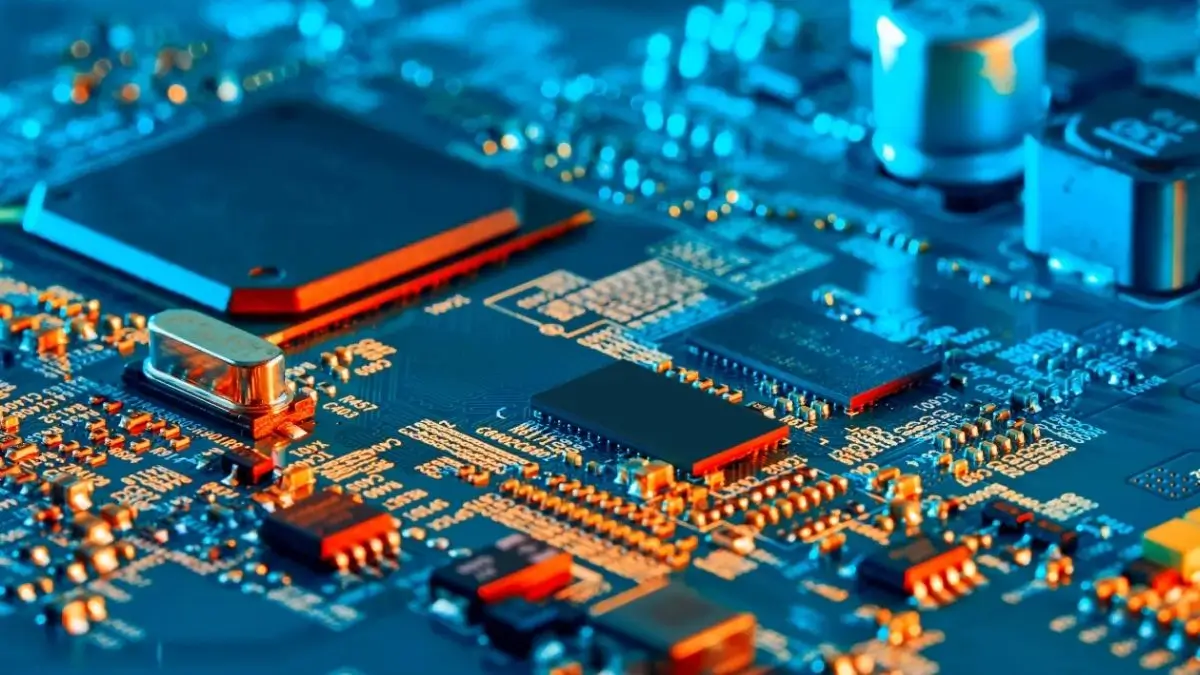
The Government of India has notified the launch of the Semicon 2.0, wherein the government will spend ₹1.27 lakh crore on the expansion of the ecosystem of semiconductors manufacturing and designing in the country. This scheme has been launched on 31st August 2026 and is an extension of the previous Semicon India Programme with the objective of positioning India within the global semiconductor value chain. Through this initiative, the government plans to promote activities such as wafer fabrication and chip manufacturing to packaging, equipment, research and talent development.
What Is Semicon 2.0?
This is the latest step taken by the Indian government for the construction of the semiconductor ecosystem in the country.
As per the Ministry of Electronics and Information Technology, this scheme will give financial and infrastructure support in the areas of,
- Semiconductor designing
- Wafer fabrication
- Packaging
- Equipment and materials
- Research and development
- Talent development
This scheme will work on the basis of six pillars and ten categories.
India Eyes Larger Presence in Global Semiconductors Market
According to the Union Electronics and IT Minister Ashwini Vaishnaw, India will be able to capture 10% of the market of the global semiconductor industry within the upcoming years.
The larger goal is to make India an integral part of the global semiconductor chain, where international players will use India for manufacturing and designing of their products.
The government expects that India’s pool of talent, policy certainty, and better ease of doing business will draw interest in investments into semiconductor industry.
Semiconductor Talent to be Further Developed
The skill development is also an important component of Semicon 2.0.
Within four years, India has trained 85,000 semiconductor engineers, which was the original target for 10 years. In addition, a new goal is formulated to train another one lakh semiconductor engineers.
The program has been expanded and now reaches out students from not only leading technology cities. The students of Tier II and Tier III cities have designed already more than 250 chips.
Project Implementation and Job Creation
The government has pointed out the speed with which projects under Semicon 1.0 have been approved from groundbreaking to commercial production.
In one case, the start of commercial production occurred in 13 months from groundbreaking. Approval for different projects was also received in 200 days, 150 days and even 90 days.
The developing ecosystem for semiconductors is expected to create around 50,000-60,000 direct jobs, apart from indirect employment through other industries.
For how many years will the Semicon 2.0 last?
The projects under Semicon 2.0 will have a tenure of six years generally.
This scheme will be open for applications for three years, giving the industries a chance to get the scheme for their semiconductor projects.
Implementation of the Scheme by India Semiconductor Mission (ISM)
India Semiconductor Mission (ISM) will be the nodal agency for Semicon 2.0.
It will invite the application, perform technical and financial evaluation, recommend the applicants and also help in the execution of the projects. It can implement the design and deployment categories with help from C-DAC.
ISM may also implement semiconductor deep-tech awards starting from 2026.








 Indian Standard Time Rules 2026 Notified...
 India Records Nearly 80% Drop in Malaria...
 PM Jan Dhan Yojana Completes 12 Years: 5...