
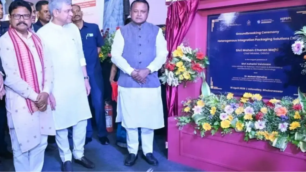
To strengthen the county’s semi-conductor system the foundation stone for the India’s first advanced 3D semiconductor packaging unit was laid in the State of Odisha on the April 19, 2026. This unit is located at the Info Valley and this project marks the major leap in India’s journey towards the self-reliance in the high end electronics manufacturing. With the investment of about the ₹2,000 crore this initiative is set to boost the cutting-edge sectors like the Artificial Intelligence, 5G, defense electronics and the high-performance computing.
India’s First 3D Chip Packaging Facility
The project, set to be developed by the 3D Glass Solutions through its Indian arm HIPSPL. It will introduce the advanced 3D heterogeneous integration (3DHI) packaging technology in India for the first time.
The foundation stone for the unit was laid in the presence of honorable Chief Minister of State Mohan Charan Majhi and The Union Minister of Ashwini Vaishnaw.
This facility will enable the next-generation chip packaging technologies and it will strengthen the India’s position in the global semiconductor value chain along with it to reduce dependence on the imports in critical technology sectors.
Odisha Emerging as the Semiconductor and IT Hub
Odisha is rapidly transforming from the mineral-based economy to the technology-driven growth centre. The state is now to becoming the focal point for semiconductor investments under the India Semiconductor Mission.
According to the government,
Odisha is the only state in India which will host the both a compound semiconductor fabrication unit and a 3D glass substrate packaging facility and it will make it a unique hub for the advanced electronics manufacturing.
This shift is expected to attract the global tech players, generate large-scale employment and it will position Odisha as a key contributor to India’s digital economy.
Investment, Capacity and Production Targets
The project involves the total investment of approximately ₹1,943 crore and it includes the central and state government support.
Once this unit get operational this facility is expected to,
- Produce around the 70,000 glass panels annually will manufacture 50 million assembled units and deliver the nearly 13,000 advanced 3DHI modules.
- Also the commercial production is scheduled to begin by the August 2028 with full-scale production targeted by 2030.
Alignment With Atmanirbhar Bharat Vision
To make the country’s self-reliant in the semiconductor and electronics manufacturing this project aligns with the Atmanirbhar Bharat vision.
India has marks the significant achievement in electronics production by becoming the,
- The second-largest mobile phone manufacturer in the world and it became the top exporter in 2025.
- This new facility will further strengthens the country’s efforts to build the robust domestic semiconductor ecosystem and it will reduce the reliance on imports and enhancing strategic autonomy.


 Karnataka Announces India's First Govern...
 Ladakh to Get Autonomous Hill Councils i...
 Gujarat's Unjha Cumin and Fennel Receive...